

5-inch Self-Supporting Diamond Wafer! Hardness Reaches 208.3 GPa
Dec 17, 2025
Leave a message
5-inch Self-Supporting Diamond Wafer! Hardness Reaches 208.3 GPa
Diamond, as the hardest material in nature, has important applications in ultra-precision machining, semiconductors, and aerospace. Traditional high-temperature and high-pressure methods for diamond synthesis suffer from limitations in size, the presence of binders, and difficulty in achieving hardness exceeding that of natural diamonds. While recent advancements in nanostructure design (such as nanotwinning) have significantly improved hardness, sample sizes are typically only in the millimeter range, and the synthesis conditions are extreme, making it difficult to achieve large-scale production of inch-sized, binder-free, ultra-hard diamonds. Although chemical vapor deposition (CVD) technology has the potential to produce large-sized diamonds, its hardness has long been difficult to exceed 200 GPa. Therefore, developing a new method for the controlled preparation of large-sized, ultra-hard diamonds has become an urgent need in this field.
A research team led by Li Chengming and Liu Jinlong from the University of Science and Technology Beijing and Lu Yang from the University of Hong Kong published a research paper titled "Inch-scale ultrahard diamond wafer with 200 GPa hardness via high-frequency pulsed local non-equilibrium growth" in the journal Nature Communications.
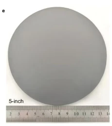
Through a self-developed microwave plasma chemical vapor deposition system, the research team introduced a high-frequency cyclic pulsed nitrogen doping strategy to achieve local non-equilibrium control during the diamond growth process, successfully preparing a self-supporting ultra-hard diamond wafer with a diameter of 5 inches and a thickness of approximately 3 millimeters. The wafer's Vickers hardness reached 208.3 GPa, comparable to that of previously reported nanotwinned diamonds, and its wear resistance was approximately 7 times that of traditional polycrystalline diamonds. High-resolution transmission electron microscopy and other characterization techniques revealed the formation of a high-density three-dimensional interwoven stacking fault network (density reaching 4.3 × 10¹² cm⁻²) within the wafer, and elucidated the microscopic mechanism by which nitrogen doping reduces the stacking fault formation energy, thereby enhancing hardness. This work provides a new approach for the large-scale preparation of inch-sized ultra-hard diamonds and their applications in high-end processing fields.
This research successfully produced an ultra-hard diamond wafer with a diameter of 5 inches and a hardness of 208.3 GPa. Using a self-designed high-frequency pulsed microwave plasma chemical vapor deposition technique, and employing hydrogen, methane, nitrogen, and a small amount of oxygen as source gases, a 5-inch polycrystalline diamond substrate with a thickness of approximately 2.8 mm was first grown on a graphite substrate. Subsequently, through a high-frequency pulsed nitrogen doping process, the nitrogen gas flow time was precisely controlled in each cycle (minimum 6 seconds). By using nitrogen atoms to perturb the plasma environment, localized non-equilibrium growth conditions were created. This resulted in the formation of an ultra-high-density three-dimensional interwoven stacking fault network within the diamond, achieving excellent performance with doubled hardness and a seven-fold increase in wear resistance.
Send Inquiry